ESP32-PICO-KIT V4
chip:esp32, chip:esp32picod4
This guide shows how to get started with the ESP32-PICO-KIT V4/V4.1 mini development board.
This particular description covers ESP32-PICO-KIT V4 and V4.1. The difference is the upgraded USB-UART bridge from CP2102 in V4 with up to 1 Mbps transfer rates to CP2102N in V4.1 with up to 3 Mbps transfer rates.
What You Need
ESP32-PICO-KIT mini development board <get-started-pico-kit-v4-board-front>{.interpreted-text role="ref"}- USB 2.0 A to Micro B cable
- Computer running Windows, Linux, or macOS
Overview
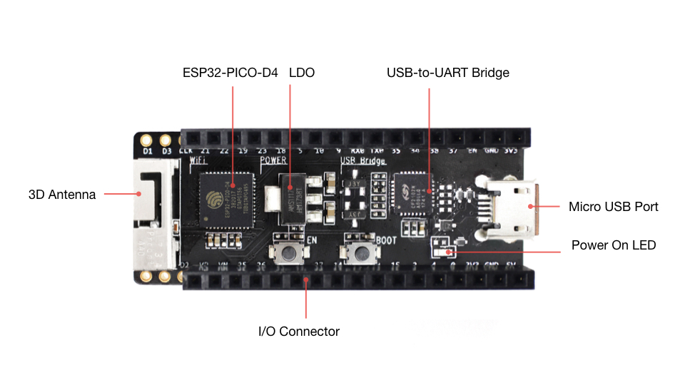
ESP32-PICO-KIT is an ESP32-based mini development board produced by Espressif.
The core of this board is ESP32-PICO-D4 - a System-in-Package (SiP) module with complete Wi-Fi and Bluetooth functionalities. Compared to other ESP32 modules, ESP32-PICO-D4 integrates the following peripheral components in one single package, which otherwise would need to be installed separately:
- 40 MHz crystal oscillator
- 4 MB flash
- Filter capacitors
- RF matching links
This setup reduces the costs of additional external components as well as the cost of assembly and testing and also increases the overall usability of the product.
The development board features a USB-UART Bridge circuit which allows developers to connect the board to a computer's USB port for flashing and debugging.
All the IO signals and system power on ESP32-PICO-D4 are led out to two rows of 20 x 0.1" header pads on both sides of the development board for easy access. For compatibility with Dupont wires, 2 x 17 header pads are populated with two rows of male pin headers. The remaining 2 x 3 header pads beside the antenna are not populated. These pads may be populated later by the user if required.
Note
- There are two versions of ESP32-PICO-KIT boards, respectively with male headers and female headers. In this guide, the male header version is taken as an example.
- The 2 x 3 pads not populated with pin headers are connected to the flash memory embedded in the ESP32-PICO-D4 SiP module. For more details, see module's datasheet in Related Documents.
Functionality Overview
The block diagram below shows the main components of ESP32-PICO-KIT and their interconnections.
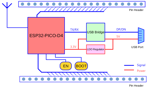
Functional Description
The following figure and the table below describe the key components, interfaces, and controls of the ESP32-PICO-KIT board.
Below is the description of the items identified in the figure starting from the top left corner and going clockwise.
Key Component Description
ESP32-PICO-D4 Standard ESP32-PICO-D4 module soldered to the ESP32-PICO-KIT board. The complete ESP32 system on a chip (ESP32 SoC) has been integrated into the SiP module, requiring only an external antenna with LC matching network, decoupling capacitors, and a pull-up resistor for EN signals to function properly.
LDO 5V-to-3.3V Low dropout voltage regulator (LDO).
USB-UART bridge Single-chip USB-UART bridge: CP2102 in V4 provides up to 1 Mbps transfer rates and CP2102N in V4.1 offers up to 3 Mbps transfers rates.
Micro USB Port USB interface. Power supply for the board as well as the communication interface between a computer and the board.
5V Power On LED This red LED turns on when power is supplied to the board. For details, see the schematics in Related Documents.
I/O All the pins on ESP32-PICO-D4 are broken out to pin headers. You can program ESP32 to enable multiple functions, such as PWM, ADC, DAC, I2C, I2S, SPI, etc. For details, please see Section Pin Descriptions.
BOOT Button Download button. Holding down Boot and then pressing EN initiates Firmware Download mode for downloading firmware through the serial port.
EN Button Reset button.
Power Supply Options
There are three mutually exclusive ways to provide power to the board:
- Micro USB port, default power supply
- 5V / GND header pins
- 3V3 / GND header pins
Warning
The power supply must be provided using one and only one of the options above, otherwise the board and/or the power supply source can be damaged.
Pin Descriptions
The two tables below provide the Name and Function of I/O header pins on both sides of the board, see get-started-pico-kit-v4-board-front. The pin numbering and header names are the same as in the schematic given in Related Documents.
Header J2
+-----+-------------------+------+--------------------------+ | No. | Name | Type | Function | +=====+===================+======+==========================+ | 1 | FLASH_SD1 (FSD1) | I/O | | GPIO8, SD_DATA1, | | | | | SPID, HS1_DATA1 | | | | | (See 1) <get-s | | | | | tarted-pico-kit-v4-pin-n | | | | | otes>{.interpreted-text | | | | | role="ref"} , U2CTS | +-----+-------------------+------+--------------------------+ | 2 | FLASH_SD3 (FSD3) | I/O | | GPIO7, SD_DATA0, | | | | | SPIQ, HS1_DATA0 | | | | | (See 1) <get-s | | | | | tarted-pico-kit-v4-pin-n | | | | | otes>{.interpreted-text | | | | | role="ref"} , U2RTS | +-----+-------------------+------+--------------------------+ | 3 | FLASH_CLK (FCLK) | I/O | | GPIO6, SD_CLK, | | | | | SPICLK, HS1_CLK | | | | | (See 1) <get-s | | | | | tarted-pico-kit-v4-pin-n | | | | | otes>{.interpreted-text | | | | | role="ref"} , U1CTS | +-----+-------------------+------+--------------------------+ | 4 | IO21 | I/O | | GPIO21, VSPIHD, | | | | | EMAC_TX_EN | +-----+-------------------+------+--------------------------+ | 5 | IO22 | I/O | | GPIO22, VSPIWP, U0RTS, | | | | | EMAC_TXD1 | +-----+-------------------+------+--------------------------+ | 6 | IO19 | I/O | | GPIO19, VSPIQ, U0CTS, | | | | | EMAC_TXD0 | +-----+-------------------+------+--------------------------+ | 7 | IO23 | I/O | | GPIO23, VSPID, | | | | | HS1_STROBE | +-----+-------------------+------+--------------------------+ | 8 | IO18 | I/O | | GPIO18, VSPICLK, | | | | | HS1_DATA7 | +-----+-------------------+------+--------------------------+ | 9 | IO5 | I/O | | GPIO5, VSPICS0, | | | | | HS1_DATA6, | | | | | EMAC_RX_CLK | +-----+-------------------+------+--------------------------+ | 10 | IO10 | I/O | | GPIO10, SD_DATA3, | | | | | SPIWP, HS1_DATA3, | | | | | U1TXD | +-----+-------------------+------+--------------------------+ | 11 | IO9 | I/O | | GPIO9, SD_DATA2, | | | | | SPIHD, HS1_DATA2, | | | | | U1RXD | +-----+-------------------+------+--------------------------+ | 12 | RXD0 | I/O | | GPIO3, U0RXD | | | | | (See 3) <get-s | | | | | tarted-pico-kit-v4-pin-n | | | | | otes>{.interpreted-text | | | | | role="ref"} , | | | | | CLK_OUT2 | +-----+-------------------+------+--------------------------+ | 13 | TXD0 | I/O | | GPIO1, U0TXD | | | | | (See 3) <get-s | | | | | tarted-pico-kit-v4-pin-n | | | | | otes>{.interpreted-text | | | | | role="ref"} , | | | | | CLK_OUT3, EMAC_RXD2 | +-----+-------------------+------+--------------------------+ | 14 | IO35 | I | | ADC1_CH7, RTC_GPIO5 | +-----+-------------------+------+--------------------------+ | 15 | IO34 | I | | ADC1_CH6, RTC_GPIO4 | +-----+-------------------+------+--------------------------+ | 16 | IO38 | I | | GPIO38, ADC1_CH2, | | | | | RTC_GPIO2 | +-----+-------------------+------+--------------------------+ | 17 | IO37 | I | | GPIO37, ADC1_CH1, | | | | | RTC_GPIO1 | +-----+-------------------+------+--------------------------+ | 18 | EN | I | | CHIP_PU | +-----+-------------------+------+--------------------------+ | 19 | GND | P | | Ground | +-----+-------------------+------+--------------------------+ | 20 | VDD33 (3V3) | P | | 3.3V power supply | +-----+-------------------+------+--------------------------+
Header J3
+-----+-------------------+------+--------------------------+ | No. | Name | Type | Function | +=====+===================+======+==========================+ | 1 | FLASH_CS (FCS) | I/O | | GPIO16, HS1_DATA4 | | | | | (See 1) <get-s | | | | | tarted-pico-kit-v4-pin-n | | | | | otes>{.interpreted-text | | | | | role="ref"} , U2RXD, | | | | | EMAC_CLK_OUT | +-----+-------------------+------+--------------------------+ | 2 | FLASH_SD0 (FSD0) | I/O | | GPIO17, HS1_DATA5 | | | | | (See 1) <get-s | | | | | tarted-pico-kit-v4-pin-n | | | | | otes>{.interpreted-text | | | | | role="ref"} , U2TXD, | | | | | EMAC_CLK_OUT_180 | +-----+-------------------+------+--------------------------+ | 3 | FLASH_SD2 (FSD2) | I/O | | GPIO11, SD_CMD, | | | | | SPICS0, HS1_CMD | | | | | (See 1) <get-s | | | | | tarted-pico-kit-v4-pin-n | | | | | otes>{.interpreted-text | | | | | role="ref"} , U1RTS | +-----+-------------------+------+--------------------------+ | 4 | SENSOR_VP (FSVP) | I | | GPIO36, ADC1_CH0, | | | | | RTC_GPIO0 | +-----+-------------------+------+--------------------------+ | 5 | SENSOR_VN (FSVN) | I | | GPIO39, ADC1_CH3, | | | | | RTC_GPIO3 | +-----+-------------------+------+--------------------------+ | 6 | IO25 | I/O | | GPIO25, DAC_1, | | | | | ADC2_CH8, RTC_GPIO6, | | | | | EMAC_RXD0 | +-----+-------------------+------+--------------------------+ | 7 | IO26 | I/O | | GPIO26, DAC_2, | | | | | ADC2_CH9, RTC_GPIO7, | | | | | EMAC_RXD1 | +-----+-------------------+------+--------------------------+ | 8 | IO32 | I/O | | 32K_XP | | | | | (See 2a) <get-s | | | | | tarted-pico-kit-v4-pin-n | | | | | otes>{.interpreted-text | | | | | role="ref"} , | | | | | ADC1_CH4, TOUCH9, | | | | | RTC_GPIO9 | +-----+-------------------+------+--------------------------+ | 9 | IO33 | I/O | | 32K_XN | | | | | (See 2b) <get-s | | | | | tarted-pico-kit-v4-pin-n | | | | | otes>{.interpreted-text | | | | | role="ref"} , | | | | | ADC1_CH5, TOUCH8, | | | | | RTC_GPIO8 | +-----+-------------------+------+--------------------------+ | 10 | IO27 | I/O | | GPIO27, ADC2_CH7, | | | | | TOUCH7, RTC_GPIO17 | | | | | | EMAC_RX_DV | +-----+-------------------+------+--------------------------+ | 11 | IO14 | I/O | | ADC2_CH6, TOUCH6, | | | | | RTC_GPIO16, MTMS, | | | | | HSPICLK, | | | | | | HS2_CLK, SD_CLK, | | | | | EMAC_TXD2 | +-----+-------------------+------+--------------------------+ | 12 | IO12 | I/O | | ADC2_CH5, TOUCH5, | | | | | RTC_GPIO15, MTDI | | | | | (See 4) <get-s | | | | | tarted-pico-kit-v4-pin-n | | | | | otes>{.interpreted-text | | | | | role="ref"} , HSPIQ, | | | | | | HS2_DATA2, SD_DATA2, | | | | | EMAC_TXD3 | +-----+-------------------+------+--------------------------+ | 13 | IO13 | I/O | | ADC2_CH4, TOUCH4, | | | | | RTC_GPIO14, MTCK, | | | | | HSPID, | | | | | | HS2_DATA3, SD_DATA3, | | | | | EMAC_RX_ER | +-----+-------------------+------+--------------------------+ | 14 | IO15 | I/O | | ADC2_CH3, TOUCH3, | | | | | RTC_GPIO13, MTDO, | | | | | HSPICS0 | | | | | | HS2_CMD, SD_CMD, | | | | | EMAC_RXD3 | +-----+-------------------+------+--------------------------+ | 15 | IO2 | I/O | | ADC2_CH2, TOUCH2, | | | | | RTC_GPIO12, HSPIWP, | | | | | | HS2_DATA0, SD_DATA0 | +-----+-------------------+------+--------------------------+ | 16 | IO4 | I/O | | ADC2_CH0, TOUCH0, | | | | | RTC_GPIO10, HSPIHD, | | | | | | HS2_DATA1, SD_DATA1, | | | | | EMAC_TX_ER | +-----+-------------------+------+--------------------------+ | 17 | IO0 | I/O | | ADC2_CH1, TOUCH1, | | | | | RTC_GPIO11, CLK_OUT1 | | | | | | EMAC_TX_CLK | +-----+-------------------+------+--------------------------+ | 18 | VDD33 (3V3) | P | | 3.3V power supply | +-----+-------------------+------+--------------------------+ | 19 | GND | P | | Ground | +-----+-------------------+------+--------------------------+ | 20 | EXT_5V (5V) | P | | 5V power supply | +-----+-------------------+------+--------------------------+
Note
- This pin is connected to the flash pin of ESP32-PICO-D4.
- 32.768 kHz crystal oscillator: a) input, b) output.
- This pin is connected to the pin of the USB bridge chip on the board.
- The operating voltage of ESP32-PICO-KIT's embedded SPI flash is 3.3 V. Therefore, the strapping pin MTDI should hold bit zero during the module power-on reset. If connected, please make sure that this pin is not held up on reset.
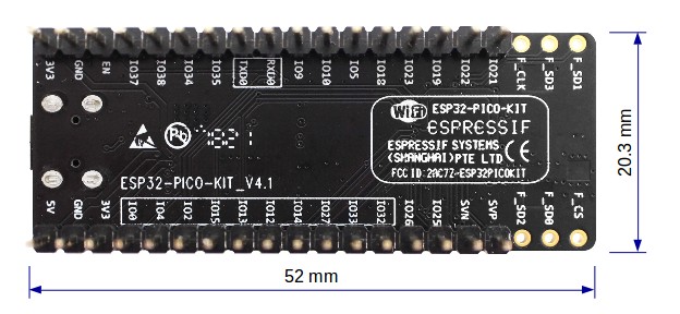
Pin Layout
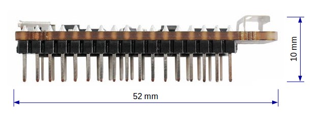
Board Dimensions
The dimensions are 52 x 20.3 x 10 mm (2.1" x 0.8" x 0.4").
For the board physical construction details, please refer to its Reference Design listed below.
Related Documents
- ESP32-PICO-KIT V4 schematic (PDF)
- ESP32-PICO-KIT V4.1 schematic (PDF)
- ESP32-PICO-KIT Reference Design containing OrCAD schematic, PCB layout, gerbers and BOM
- ESP32-PICO-D4 Datasheet (PDF)
Configurations
All of the configurations presented below can be tested by running the following commands:
 ./tools/configure.sh esp32-pico-kit:<config_name>
 make flash ESPTOOL_PORT=/dev/ttyUSB0 -j
Where <config_name> is the name of board configuration you want to use, i.e.: nsh, buttons, wifi... Then use a serial console terminal like picocom configured to 115200 8N1.
nsh
Basic NuttShell configuration (console enabled in UART0, exposed via USB connection by means of CP2102 converter, at 115200 bps).